
Successful international workshop on photonic integrated circuits in Berlin – thin-film technologies as the key to industrial PIC architectures
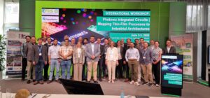
Berlin, June 2026 – On 2 and 3 June 2026, the Fraunhofer Heinrich Hertz Institute (HHI) in Berlin hosted the international workshop “Photonic Integrated Circuits – Mapping Thin-Film Processes to Industrial Architectures”, organised by the European Thin Film Society (EFDS). The event brought together leading experts from industry and research across the entire value chain of integrated photonics. The focus was on thin-film technologies as a key connecting element for the development, integration and scaling of future photonic systems.
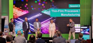
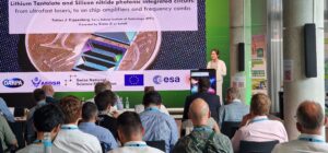
The high-calibre programme covered a wide range of topics – from materials and thin-film processes, through design and integration, to industrial manufacturing and applications in telecommunications, data centres, sensor technology and quantum technologies. The content spanned the entire technological chain: from thin-film deposition challenges for SiN waveguides at IMS CHIPS and reactively sputtered ScAlN and BTO layers for electro-optical modulators at Fraunhofer FEP, to co-packaged optics for scaling AI computing infrastructures at IBM, as well as photonic platforms for quantum technologies from QuiX and Linq Photonics.
The presentations were notable for their high technical quality and their relevance to current industrial developments. Particular mention should be made of the in-depth Q&A sessions and discussions that followed the presentations, which highlighted the participants’ keen interest and facilitated a lively exchange between the worlds of research and industry. The programme was complemented by poster presentations, which offered further insights into ongoing research and development work.
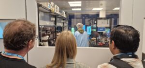
The Fraunhofer HHI acted as host not only a modern and open environment in the heart of Berlin, but offered the participants an exclusive lab tour a21> on the second day of the event fascinating insights into current research activities and technological infrastructures. The light-filled premises and the attractive setting created ideal conditions for intensive networking and professional exchange.
Special thanks go to Fraunhofer HHI and the entire on-site organising team for their excellent support, professional organisation and warm hospitality. The EFDS would also like to thank the programme committee – Andreas Ehrhardt (Photonics BW e. V.), Matthias Hutter (Fraunhofer IZM), Silvia Schwyn-Thöny (Evatec AG), Christian Schindler (Bühler Alzenau GmbH) and Andreas Salzinger (Photonics BW e.V.) – for their close, constructive collaboration, which played a key role in shaping a balanced and high-quality programme.
In addition to the technical content, the workshop offered numerous opportunities for personal exchange, including among other things during setting of a joint dinner in a pleasant atmosphere. The event was characterised by overall a high level of interactivity, strong practical relevance and excellent networking opportunities in particular.
The successful delivery of the workshop provided a significant impetus for further dialogue within the international PIC community. The EFDS remains committed to creating platforms for interdisciplinary exchange and to strengthening collaboration between materials science, process development and industrial applications in the field of thin-film technologies on a long-term basis.
 |
 |
 |
 |
 |
 |


